|
|
|
Research
COMMUNICATION AND RF DESIGN
Name: Dr. Pranoti S.Bansode-Gaikwad
Designation: Assistant Professor
Specialized Area: RF Design, Microwaves and Antenna, 5G Systems.
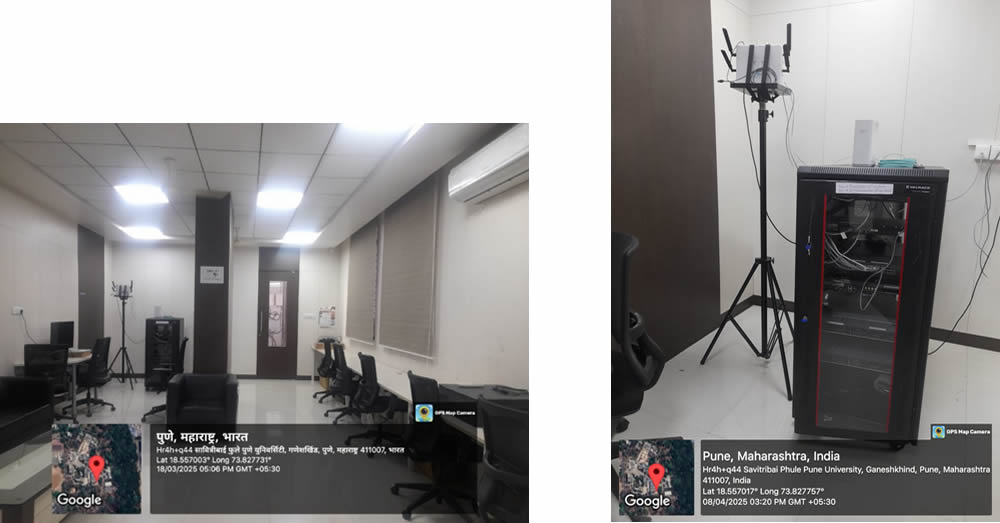
5G Use Case Laboratory
The 5G Use Case Lab grant for Higher Educational institutions is set up in collaboration with Dr. Babasaheb Ambedkar Technological University, supported by the Department of Telecommunication & TCIL, Govt of India.
The vision of the lab is to empower students and researchers with hands-on experience in 5G technologies, contributing to the nation’s goal of becoming a global leader in telecom innovation.
The lab aims to foster research, innovation, and development in the domain of 5G technology and its practical applications across industries.
Focus Areas of the lab is 5G Network Design and Deployment, Internet of Things (IoT) over 5G, AI/ML for 5G, mmWave Communications, Smart Cities, Healthcare, Agriculture, and Industry 4.0 Applications.
The lab offers the various cutting-edge facilities and tools for experimentation and development in 5G technologies such as Smart camera, 5G Drone, IoT sensors. etc.
RF System& Antenna Design lab
Department has state of the art RF equipment for RF circuit design with which different types of Antenna, Filters, RF circuits, LNA’s, Mixers etc. have been developed for the frequencies ranging
from KHz to GHz. Different simulation software’s like AWR (Applied Wave Research), and 4NEC2 are available. Vector Network Analyzer (Upto 3 GHz), Spectrum Analyzer (Upto 6GHz), RF function Generator
(Upto 3 GHz), Waveform generator, MSO (Mixed Domain Oscilloscope), DSO(Digital Signal Oscilloscope) are also present. The lab has different types of antennas simulated, designed,
fabricated by students indigenously using the various facilities in the lab.
Ongoing Projects in RF lab:
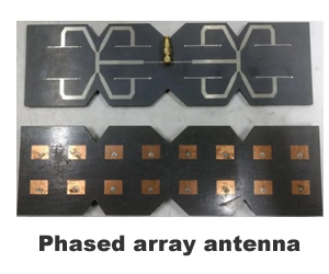
- Design, Simulation and Fabrication of Phased array antenna in LTCC (Low temperature co-fired Ceramic). Pranoti S. Bansode.
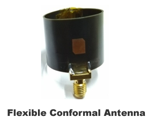
- Study of Conformal Antenna: ARDE CARS Project, Mr. Swapnil Narke.
- Vector network analyzer (VNA) (Agilent E5062A).
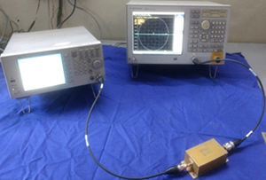
A network analyzer is an instrument that measures the network parameters of electrical networks. Today, network analyzers commonly measure s–parameters because reflection
and transmission of electrical networks are easy to measure at high frequencies, but there are other network parameter sets such as y-parameters, z-parameters, and h-parameters.
Network analyzers are often used to characterize two-port networks such as amplifiers and filters, but they can be used on networks with an arbitrary number of ports.
Signal generator (Agilent N9310A)
RF Signal generator is used to generate the RF signal. The frequency range of Signal generator is 9 KHz to 3 GHz. It has tow port output one is LF (Low frequency output)
and RF (Radio frequency output).It has provide Maximum 4W power at the output.
Spectrum analyzer (Agilent CSA Spectrum Analyzer)
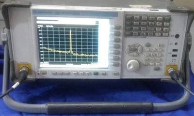
A spectrum analyzer measures the power of the spectrum of known and unknown signals. The frequency range of Spectrum analyzer is from (100 KHz to 6 GHz).
It gives the information of S-Parameters and power measurement of signal.
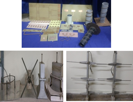
Antennas
In RF lab students have designed,Simulated and fabricated different types of planer and wire antennas. Photgraph shows some antennas like
patch antennas,array antennas,phase array antenna,horn antenna,Helix antenna,Smart antenna,cantenna,Cross- dipole,Log priodic antennas designed.
Research Projects Completed
- Microstrip patch array antenna for Low cost C band Micro SAR funded by DRDO in 2010
- Conformal Antenna Design for Onboard GPS Receiver on Spinning Projectile consultancy project by Zeus Numerix Pvt. Ltd. in 2023.
Ongoing Research Projects
- Dual Purpose Tri Band Proximity Coupled Microstrip Patch array antenna funded by ARDE in 2021
Mechatronics Lab
Faculty Incharge: Dr. Shamal L. Chinke
Designation: Assistant Professor
Specialized Area: Embedded Systems, Defence Electronics, Shock and Blast Mitigation.
Research and Development Activities in Mechatronics Lab
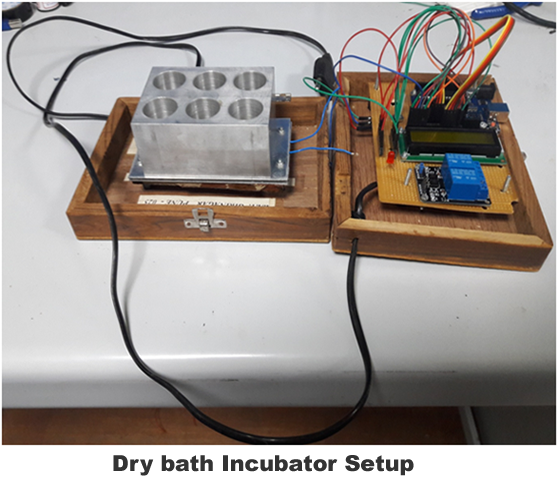
- Design and Development of Dry bath Incubator for laboratory application
- Military purpose, man portable, fully integrated, dual chargeable, additively manufactured, real time, high performance, ballistic chronograph: design, development, and system engineering
- Design and development of virtual laboratory experimental setup to study the characteristics of solar cell
The COVID-19 pandemic has profoundly impacted education in India and abroad. The studies of students studying science impacted heavily because science has to be learned through
experimentation and the students were unable to perform science experiments since during the pandemic labs of many universities and educational institutes were closed.
In order to address this issue many institutes came with the concept of performing the simulated lab experiments but students were not completely happy since they were just able to perform the simulated
experiments not actual experiments. Then to address this problem one of the effective method is the use of virtual experimentation. Designing and development of virtual laboratory
experimental setups that enables the students to perform the experiments from their home and get them the closure feel of performing the experiments practically.
The present paper deals with design and development of one of such virtual laboratory experiment aimed at studying the characteristics of solar cell.
The solar cell experiment was designed using LabVIEW software interfaced with microcontroller to vary the Intensity of light and load resistance.
The web pages and user interface have been designed using Microsoft Visual Studio and HTML software. The current-voltage (I-V) and power-voltage (P-V) characteristics of the solar cell have been studied.
This virtual experiment provides a powerful tool for education and research, allowing users to explore the behaviour of solar cells in a controlled, interactive environment.
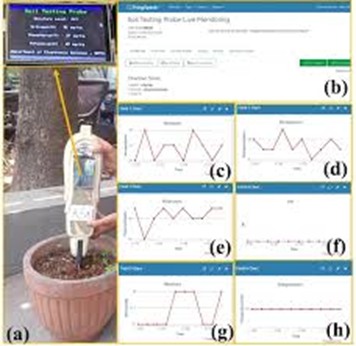
- Advanced soil testing probe: design, development and system engineering
Soil testing plays a vital role in achieving optimal plant growth, maintaining soil health, protecting the environment, and ensuring cost-effective and sustainable agricultural practices.
However, the traditional soil testing methods face several problems since it involves labour-intensive, time consuming, cost associated with transportation and handling.
Further the soil properties can vary widely within a short distance, so it becomes difficult to have representative samples that accurately reflect the entire area with distance.
Hence, there was a need for design and development of advanced soil testing probes that can be used at the field locations for rapid testing and having accuracy, efficiency and cost effectiveness.
However not much work is reported on advancement in soil testing probes. The present paper deals with the design and development of an advanced soil testing probe for in field monitoring of the critical soil parameters
such as nitrogen (N), phosphorus (P), potassium (K), pH, moisture, and temperature. The system is developed with STM32 microcontroller and ESP32 Wi-Fi interface and the Math-Works ThingSpeak
Internet of Things (IoT) cloud platform to provide real-time data collection, transmission, and analysis. The system is equipped with calibrated sensors, collects data on soil nutrient levels and environmental conditions,
transmitting this information via Wi-Fi to the ThingSpeak cloud for continuous monitoring. Users can access and visualize the data through ThingSpeak’s dashboards, facilitating an intuitive understanding of soil health.
The field-testing results indicates that stable nitrogen, phosphorus, and potassium levels, consistent pH, and moisture content, with expected temperature variations, highlighting the reliability and accuracy of the system.
This real-time data enables optimized fertilization, irrigation, and crop management practices, contributing to improved soil health and agricultural productivity.
This advanced soil testing probe represents a significant step towards precision agriculture, offering farmers and agronomists a powerful tool for enhancing crop yield and sustainability.
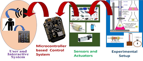
- Design and Development of Experimental Setups for Blind and Low Vision Students Imagining life without vision is very difficult and the people who are facing problems like blindness and vision impairments have to face
numerous challenges. However, in last few decades, number of initiatives are taken by people, social welfare organisations, CSR initiatives with encouragement and support from government has ted to establishment
of number of schools to providing education to blinds and people with low vision. It is very challenging to provide education to blinds, especially subject like Science which must be learned through experimentation,
as experimentation may attract the interest of students towards that subject and improve in their understanding also enrich them with skills as well as add an experience of handling new things.
Looking at the current scenario, in most cases assistants performs the practical experiments on instruction of blinds as with the current practical setups/models, the experiments cannot be performed by blinds alone.
one can easily identify the need for design and development of an accessible, interactive and user-friendly experimental setups, 3D models for performing science experiments by these students.
The current proposal deals with the setting up a science laboratory by design and development of such experimental setups with the help of which the differently abled students can explore science.
The targeted users are the students from Class VIII to Class XII. The experimental setups will be made with the state of the art, use of the upcoming technologies such as Embedded Systems and IoT,
Artificial Intelligence and Machine Learning, Cloud computing etc. As of now we have prepared 2 such experiments for demonstration, Simple Pendulum and Identification of Halide. With the tie up from industry experimental
setups will be modified to fulfil and meet the standards of the reliability and safety
Space based Electric and Magnetic Sensor (SEAMS) Lab
Faculty Incharge: Dr. Aditee C. Joshi
Co-PI Prof. Damayanti C. Gharpure
Specialized Area: Digital system design, RF front end design, Radio astronomy Instrumentation..
Facilities
- Tektronix RSA 500 A Series Portable Spectrum Analyzer
- Tektronix 3 Series MDO (2 Channel)
- N5171B-501 X-Series RF Analog Signal Generator, 9kHz to 1 GHz.
- Keysight 33600 A Waveform Generator
- Nano VNA V2 (S-A-A-2) 50 kHz-3GHz
Research Arenas
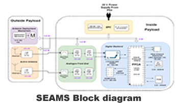
- Space Payload Design
- Front end: LNA, Filter design
- Back end: FPGA based data acquisition & signal processing.
- RF system design
Research Projects
- Establihment of Space Payload Design Center
- Origin of Payload of Project : Advisory Committee on Space of ISRO as well as the launch team of PSLV prototype model selected SEAMS-Phase I payload for the PSLV last stage orbital platform.
SPPU is the only University in India funded by ISRO to work in this frontline area
- Meeting held with Advisory Committee on Space of ISRO, Padmabhushan Pramod kale (Ex. Director SAC, ISRO Ahmedabad), Prof. S. Ananthakrishnan (Ex Director ,GMRT), Prof. Shaligram & Prof. Gharpure
proposed inception of Space Payload Design Center(SPDC) at university campus based on research excellence gained by department.
- Mission statement: To create a small focused group/ development center in SPPU, which acts in future as an excellent nodal point with a synergetic multi-disciplinary ambiance for SPPU depts and other University depts.
too to learn about the intricacies of space payload development.
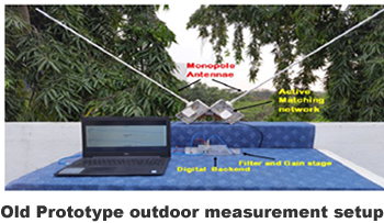
In anticipation of a Space Payload Development Center (SPDC) of the SPPU, the first task that has already been taken up, namely, the prototype design of SEAMS-Phase
I as a payload of the PS4 orbiter to study the RFI in the low earth orbit is nearing completion. It is funded by Savitribai Phule Pune University for year 2022 & likely to
be continued further before an engineering and flight model is built for launch into a low earth orbit (LEO).
-
Space based Electric and Magnetic Sensor (SEAMS) for very low frequency (0.3 to 15 MHz) radio astronomy aims at conducting sensitive measurements of the sky-averaged spectrum at very low radio frequencies (below 20 MHz).
It also characterizes radio frequency interference (RFI) from a space location in the Low Earth Orbit.
While expressing this explicit interest, we wish to draw attention to the fact that this has indeed been our first of the key targets/phases in a wider set of astronomical exploration defined/proposed in our ongoing project SEAMS.
The SEAMS frequency range (0.3 to 15 MHz) has been chosen because it is a unique range which is yet to be explored by radio astronomers, as the Earth's ionosphere is impervious to these frequencies and we need a space based platform to study this frequency range.
SEAMS has been proposed to be developed in two phases. In the first phase, we would like to locate the payload (albeit with reduced cost of components, etc.) in low earth orbit,
on the 4th stage of PSLV to study the RFI from Earth and to understand the nuances of data acquisition and analysis.
The first phase will also attempt to decipher the background Galactic Spectrum and any major solar activity as well as to give us insight into creating an interferometric array later.
In the second phase, it is proposed to locate the payload on the far side of the Moon or in the Moon-Earth L2 to avoid the RFI from Earth.
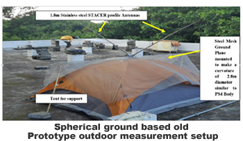
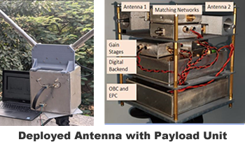
Various antenna structures and deployment mechanisms have been fabricated and experimented. The design optimization will be done with the help of experts from ISRO units.
Work on RF front end and its testing from the optimization point of view is being carried out. The FPGA back end has been designed and the prototype system is also fabricated.
Future Research Projections
We have approached ISRO unit for further testing, optimization, boxing and packaging procedures.
The next target would be the design of final development & validation of the payload for the PS4 platform under guidance from experts at ISRO.
 |
 |
 |
 |
Atharva Kulkarni
JRF
Front end design |
Sunil Pingale
Technical Assistant
Front end assembly, testing
|
Kushal Bhalerao
Project Asssistant
Back end design
FPGA based data acquisition
|
Aditi Nagulpelli
SRF
Front end design
|
 |
 |
 |
 |
Nikhil Navale
Project Associate I
Mechanical testing & antenna deployment
|
Rasika Sali
Project Associate I
Front end design
|
George N George
Project Asssistant
FPGA design manufacturing
|
Praphulla Saste
Project Asssistant
On board computer
& electronic power control system
|
 |
 |
 |
Raghuttam Hombal
Project Asssistant
Back end design
FPGA based signal processing & analysis
|
Niketan Pawar
Project Engineer
Mechanical design analysis and modelling simulation
Antenna deployment mechanism
|
Samruddhi Rohokale
Project Asssistant
Analog Front end design
LNA, RF circuit Design
|
Publications
-
SEAMS Phase I - RF Frontend for RFI measurement in LEO. Atharva Kulkarni, Rasika Sali, Aditi Nagulpelli, Nikhil Navale, D.C Gharpure and S. Ananthakrishnan. URSI - RCRS 2022, IIT Indore, India, 1 - 4 December, 2022.
-
SEAMS Phase I - Data Acquisition System and On-Board Computer. Aditi Nagulpelli*, Atharva Kulkarni, Praphull Saste, Rasika Sali, Raghuttam Hombal, and D.C. Gharpure. URSI - RCRS 2022, IIT Indore, India, 1 - 4 December, 2022.
-
Space Electric and Magnetic Sensor (SEAMS) antenna and its deployment mechanism. Nikhil Navale, Aditi Nagulpelli, Atharva Kulkarni, Rasika Sali, A.C. Joshi, D.C Gharpure and S. Ananthakrishnan. URSI - RCRS 2022, IIT Indore, India, 1 - 4 December, 2022.
-
A. Datta, D.C. Gharpure, S. Ananthakrishnan, P. Janardhan, A. Kulkarni, N. Navale, A. Nagulpelli, and R. Sali, “Space-based Electric and Magnetic Sensor (SEAMS) for very Low-frequency Radio Astronomy”. URSI GASS 2021, Rome, Italy, 28 August - 4 September 2021.
-
RF Front-End for SEAMS. Atharva Kulkarni, Sunil Pingale, Damayanti Gharpure and Subramaniam Ananthakrishnan. URSI AP-RASC 2019, New Delhi, India, 09 - 15 March 2019.
-
Borade, Rupali; Dimber, Akash; Gharpure, Damayanti; and Ananthakrishnan, S. (2018). Design and Development of FPGA-Based Spectrum Analyzer. IETE Journal of Education, 59, pp. 1-13. DOI: 10.1080/09747338.2018.1450648.
-
Borade, Rupali and Gharpure, Damayanti. (2018). FPGA Implementation of Nonparametric Power Spectrum Estimation Methods. Pages 30-35. DOI: 10.1109/CTEMS.2018.8769222.
Sensors and smart materials
Research Arenas
- Thin Film deposition and processing
- Nanomaterials based gas sensor
- Intelligent instrumentation
Magnetron sputtering, Physical vapor deposition and optical lithography room are the important facilities available in the fabrication laboratory.
For piezoelectric materials Pellet mill and piezometer system for piezomaterials characterization is also available.
The FAB Lab has a fully equipped yellow room along with clean benches and DI water facility for optical lithography purpose.
Previous Research Developments
The laboratory has a main focus on development of thin film based devices for various applications like sensors and piezoelectric transducers and masking materials.
Development of Silicon based thin/thick film microsensors is carried out in the laboratory. An in-house EBL system (lc EBLS1), around a Scanning Electron Microscope, has been developed successfully.
This system can be used to evaluate the resist, to make masks and to inspect the mask or pattern delineated in the resist. In the early stages polymers like PMMA, PTFE,
HEMA as masking materials for silicon micromachining have been investigated. Optimization of silicon nitride (Si3N4) and indium nitride (InN) for antireflection coating has been carried out.
A Si based Hall sensor is developed indigenously for use in Automobile industries for RPM measurements of the wheels. Plasma polymerized PMMA was characterized and used for application in humidity sensing material.
An indigenous system is developed for detection of radial pulse using piezoelectric transducers. A complete set up along with integrated electronics and LAB-VIEW based front end design was developed and tested.
A database is generated to classify pulse data according to different characteristics indicated by ayurvedic experts and this will be useful to study overall health of a person.
MEMS based devices were designed using Coventorware software and further studied for application in RF MEMS and acceleration sensors. Conducting polymers and composites based gas sensors
were fabricated and successfully implemented for detecting NH3, Cl2 and H2S, NO. The work has been done on deposition and characterization of polymer based thin films for application in development of SAW based sensors.
Similarly development of electrochemical sensor for NO2 monitoring along with signal conditioning is underway. A noise source based on inert gas plasma tube is developed.
Research /consultancy Projects
Development of optical disdrometer: ISRO Space Technology Cell, 2018-2022
Research Scholars
| Mr. Swapnil Narke |
Ph.D. Scholar |
 |
Conformal Microstrip Phased Array Antenna. |
| Mr. Ishaan Karnik |
Ph.D. Scholar |
 |
Design, development and performance evaluation of photo-voltaic system for variable load configuration in Indian climatic conditions. |
|
Copyright
©
University of Pune. All Rights Reserved.
|
|